Semiconductor Electroplating Systems
Solstice Series
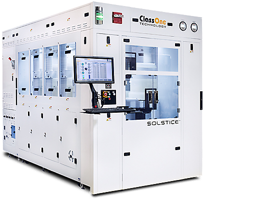
Solstice S8
Automated Electroplating Systems
Advanced, single-wafer, high-throughput ECD and Surface Preparation – with up to eight chambers
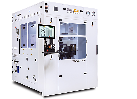
Solstice S4
Automated Electroplating Systems
Advanced, single-wafer, high-throughput ECD and Surface Preparation – with up to four chambers
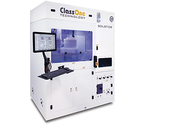
Solstice LT
Electroplating Development Systems
Semi-automated single-wafer Process
Development – with up to three chambers
Let’s Talk
We listen and respond to your unique challenges to provide the right technology at the right time and meet your manufacturing goals. Reach out, and we’ll deliver a solution.


